A real-world 8085 project
Soon after writing my text about building your own MCU/CPU project
Lewis Stockill <mstockill@aol.com> emailed me about a small 8085
system he was building as a hobby.
I helped him to debug the system a bit (via email) and he immediately
agreed that it would be a nice idea to describe the project in some
detail in the Chipdir for others to learn from.
Why use the 8085 one might ask. Well it's a straight and simple
traditional 8-bits processor with hardly any strange quirks, except
perhaps that the data bus is combined with the lower part of the address
bus to save pins. This trick is often used and you only need a one way latch
to keep the address stable while the bus is used for data in the second
halve of the memory cycle. The 8080 and even the later 8086/8088 need two
82xx series support chips, whereas the 8085 can work on it's on (except for
the latch).
The final schematics of the project
| local |
JPG file of the Autocad schematic (390 Kbyte) |
(This map doesn't seem to be downloadable from www.hitex.com/chipdir/
so you may have to get it from another mirror site.)
The last completed CAD* image of the 8085 circuit design (without
the 7-segment display).
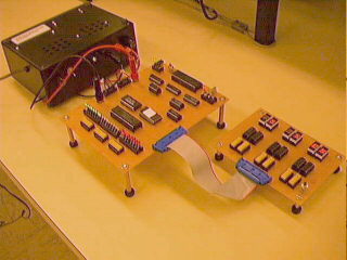
A photo of the finished project
 The completed 8085a unit along with the power supply that Lewis built
and a 7-segment display unit. The photo shows the computer in operation.
The designer at work designing
 A photo of Lewis at work, designing the project.
Tips from Lewis
Here are a few tech tips for future designers/builders of 8085 circuit:
Initially build the circuit without using CMOS* chips. If wiring
errors are encountered then it may be nearly impossible to diagnose the
circuit since erratic oscillations will most likely occur.
Once the circuit is up and running with TTL chips (LS*), then swap
out all TTL's for HCT*'s or other CMOS* equivalent IC*'s.
The circuit should run fine.
When writing code for this or any ROM/RAM chips, be careful as to
addressing. ROM and RAM are most likely of different sizes (as in the
case of this circuit (4K ROM, 2K RAM), and initializing the stack
pointer is very crucial (1800H in this case.)
Thanks for your help Jaap, and I'll keep you posted on other future
projects that may be of interest to you or others. This was a fun and
challenging project, and who knows, with all the Y2K hoopla this little
"re"-design may come in handy for some future young repair tech.
Test software
************************************
Here is a test program in assembly language that will work:


; ******* Program 4 ******************
; LED lighter with inline delay
	.ORG	0
	JMP	MAIN
MAIN	.ORG	100H
	LXI	SP,1800H
	NOP
	MVI	A,10000000B
	OUT	CTRLW
	MVI	A,7FH
LOOP	OUT	PORTA

	; save to memory
	STA	SAVE

	; read from memory
	; (need to save value in A)
	MOV	E,A
	MVI	A,0
	LXI	H,SAVE
	MOV	A,M
	OUT	PORTB
	MOV	A,E

	OUT	PORTC

	; inline delay
W2	DCR	C
	JNZ	W2
	DCR	D
	JNZ	W2
	DCR	B
	JNZ	W2

	RRC
	JMP	LOOP

	NOP
PORTA	.EQU	0
PORTB	.EQU	1
PORTC	.EQU	2
CTRLW	.EQU	3
SAVE	.EQU	1000H

	.END	100H
	.END
See also
If you haven't already, check out my short introductory text about
designing your own small processor/controller system.
A similar subject is designing your own processor using FPGA:
On that page there is also a $295 Z80 controller board that seems to be quite
complete (and open!) so if you don't feel like designing the board but only
the software, rip out the EPROM* and write your own monitor program! ;-)
www.thesis.cjb.net/ - Another group designing their own FPGA processors.


 The completed 8085a unit along with the power supply that Lewis built
and a 7-segment display unit. The photo shows the computer in operation.
 A photo of Lewis at work, designing the project.